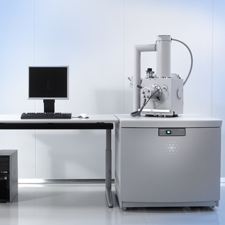
FEI Nova nanosem 230, equipped with RAITH e-beam lithography system.
The NanoSEM 230 is a field-emission scanning electron microscope (FE-SEM), which attains ultra-high resolution imaging (magnification up to 500.000x) in a digital format. The NanoSEM field-emission source allows the user to achieve high imaging resolution at a range of kV, at both low (high-resolution imaging) and high (microanalytical imaging) currents. The Nova NanoSEM 230 is fitted with ETD, TLD and LVD detectors for the detection of secondary or backscattered electrons in High or Low vacuum mode while a HELIX low vacuum detector for the detection of secondary electrons has been also fitted (best detector for high resolution imaging at Low Vacuum conditions). The system Is also equipped with a RAITH e-beam lithography system, making it capable of writing patterns down the nm scale.
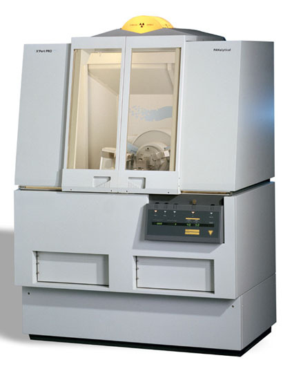
Panalytical X'pert pro
The Panalytical X’Pert Diffractometer is a highly advanced, versatile materials characterization system. Interchangeable PreFIX incident and diffracted beam optics can be configured for optimal measurement of high resolution scans, reflectivity experiments, or for in-plane diffraction. High Resolution X-ray Diffraction: High resolution x-ray diffraction is generally applied to highly ordered crystals. It is useful to examine nearly lattice matched materials or the structural perfection of materials. Reflectometry: Reflectometry is an analytical technique for investigating thin layers. In-plane diffraction: The in-plane diffraction technique measures diffracted beams nearly parallel to the sample surface and hence measures lattice planes that are (nearly) perpendicular to the sample surface. These planes are inaccessible by other techniques.
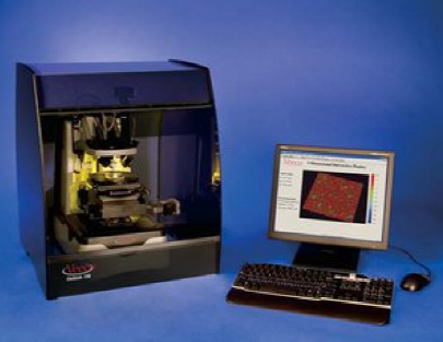
Veeco dektak 150 surface profiler
The Dektak 150 stylus profiler includes a two-axis, manual sample-positioning stage with 101.6 x 101.6 mm (4 x 4 inches) of X-Y translation, manual leveling, two-point programmable or cursor software leveling, and manual theta rotation. The instrument accommodates samples up to 90 mm (3.54 inches) thick and performs long scans of 55 mm (2.16 inches) with a maximum of 120.000 Data Points Per Scan. It provides ± 50.8 mm (2 inches) of X-Y translation as well as manual theta positioning. In addition to 50 mm (1.97 inch), 100 mm (3.94 inch), and 150 mm (5.90 inch) wafer alignment pins, the theta chuck provides three-point suspension for performing stress analysis.
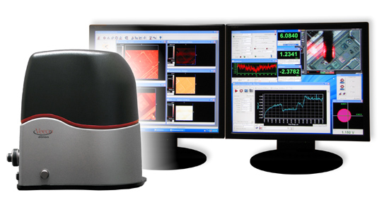
Veeco DiInnova AFM
A scanning probe microscopy AFM system that is capable of operating in contact and tapping mode, for measuring and investigating the surface topography of materials. Contact Mode: This is the most basic and straightforward AFM mode. In this case, the AFM probe tip is in constant physical contact with the sample surface. Tapping Mode: The most commonly used AFM mode for imaging soft or fragile samples. This technique maps topography by lightly tapping the sample surface with an oscillating probe tip. The system is capable of conducting large (100 μm) as well as small (5 μm) area scans.